The FW16 7840HS mainboard has a connector ( unsoldered ) labeled JUDC with 30 pins.
It is not documented anywhere.
Does anyone know what it is for?
What is the pin out?
I don’t work for Framework. As a fan of pcb layout, I can make an educated guess what it is:
J = Jumper (aka pins, connector, pads)
U = Universal or USB
D = Debug
C = Connector (yes, this is redundant with J)
That is an incredible “easter egg” find. You’ve spotted one of the rare unpopulated headers that Framework leaves on their boards for internal engineering and future-proofing.
On the Framework 16 (7840HS) mainboard, the JUDC label likely stands for “JTAG / USB Debug Connector.”
What is JUDC?
In high-end board design, “JUDC” is typically a proprietary or semi-standardized debug interface used by the factory.
-
30-Pin Count: This is the standard density for a full JTAG + SWD + Serial Console suite.
-
Function: During the EVT (Engineering Validation Test) phase, Framework engineers use this header to “unbrick” boards, flash the BIOS directly to the SPI chip, and monitor low-level CPU/EC (Embedded Controller) heartbeats before the screen even turns on.
Why is it unsoldered?
For the consumer version, Framework leaves this unpopulated for three reasons:
-
Security: Leaving a live JTAG header soldered on makes the laptop vulnerable to hardware-level “cold boot” attacks or unauthorized firmware injection.
-
Z-Height: The physical connector would add 1-2mm of height, which might interfere with the mid-plate or the tight tolerances of the Input Module system.
-
Cost: When you’re manufacturing thousands of boards, omitting a connector that 99.9% of users will never use saves a significant amount of money and reduces failure points.
Can you use it?
Unless you are a hardcore firmware developer with a J-Link or Bus Pirate, it’s best left alone. However, if you’re feeling adventurous:
-
Pinout: While not in the user manual, you can often find the traces in the Mainboard Interfaces Schematic on the Framework GitHub.
-
The “Hack”: If you ever permanently brick your BIOS (and even the “Mainboard Reset” doesn’t work), a skilled micro-solderer could technically use these pads to manually talk to the Flash chip.
Next Step for the “Hardware Geeks”: Would you like me to find the 3D CAD files for the mainboard so you can see exactly where that header sits in relation to the other components? It’s a great way to plan custom “internal” mods!
1 Like
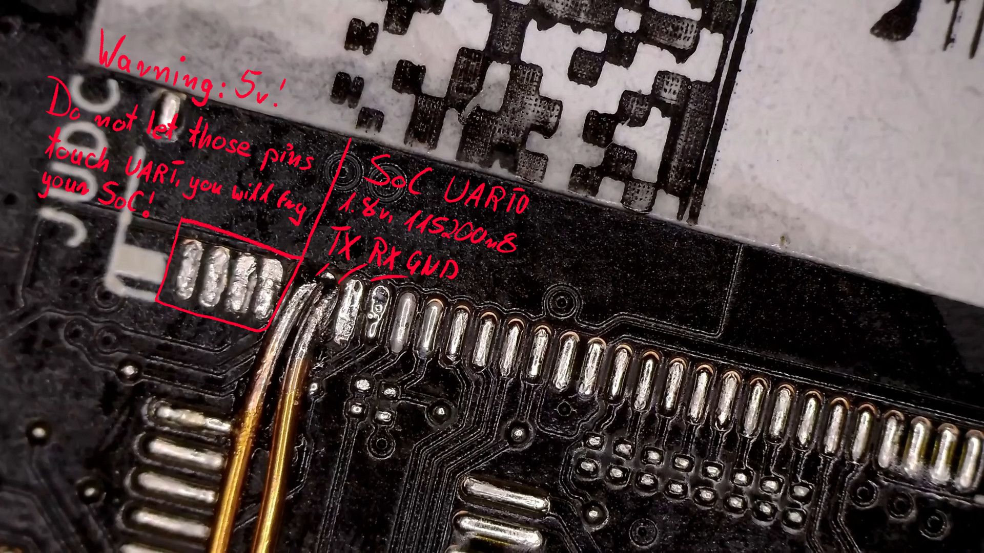
- SoC UART0
- eSPI (bus used by Embedded Controller)
- SoC JTAG (it can only be used with AMD’s software running on AMD-provided laptop connected to their VPN under a very strict NDA
I don’t think I can tell you the pinout, but please do not try to poke it with an oscilloscope or logic analyzer.
There are 5V pins right next to SoC UART, and AMD SoC uses 1.8V logic for it’s entire I/O block. If you short those pins, you will fry processor on your board.
1 Like
@ellyqw
Thank you for the info.
Do you happen to know the pin out for the JECDB connector on the FW16 7040 mainboard.
It is another unpopulated connector.
I have access to the EC console using the EC CCD. The EC CCD also gives a CPU console on the FW13, but it does not work on the FW16.
There appear to be UARTs available on various other connectors, e.g. the E-Type M.2.
Are those the same as the CPU console UART ?
The JSWDB connector is documented in the published FW schematics, and has a UART and EC console port pins.
So, I am curious if that UART is the same as the CPU console UART, or is that only available on the JUDC 30-pin connector, as you show?
Framework documented it on their git actually: GitHub - FrameworkComputer/FrameworkDebugger: Debugger Firmware Multitool · GitHub
However, it’s not fully correct in Framework 16’s case. As far as I can tell, those UART pins are connected to Cypress PD controller instead of SoC UART. Other than that, it’s correct. I assume you can re-flash the EC using JTAG/SWD pins.
All I needed was EC UART, so that’s how it looks like. It’s convenient because I don’t need to deal with PD negotiation/muxing and can do stuff like resetting the ec, powering the board on and setting fan speed without having to physically reach the machine (it’s on my desk, but it’s much more convenient to do it from the terminal) ![]()

1 Like
Thank you for that.
On the FW16, where do you connect the CPU BIOS firmware flash pins?
On many laptops on the market. One can use the EC console port to:
- Flash the EC firmware.
- Flash the PD firmware.
- Flash the CPU BIOS firmware
But, it appears that not all the above is reachable from the EC console port.
So, I am curious how to get to (3) at the moment.
We would need all 1,2 and 3 in order to come up with an “un-brickable” mod so users can recover from failed BIOS/EC/PD updates.
For example, the “un-brickable” mod on one device I worked on, did:
- Boot the EC via the serial/UART console port.
- Update the EC firmware via the UART port, using the tools provided in the booted EC image via the serial port.
- The EC then had SPI and I2C links to program the USB PD and CPU BIOS firmware, again via the EC UART port.
Do you have any example UART output from the JECDB you have connected?
I only currently have EC CCD - EC console port output, that I used when modding the EC firmware for my uses.
On many laptops on the market. One can use the EC console port to:
[…]
Flash the CPU BIOS firmware
Not in my experience (and I’ve been doing this full-time for a few years now). Usually SPI line from main flash to EC is used to recover EC/update it’s firmware (i.e with ITE EC it reads first ~128KB of flash upon power-on to check and update itself after you disconnect the battery).
Technically you’re correct and it should be possible (i.e: BMC present on servers), but I’ve never seen this in practice on a laptop.
So, I am curious how to get to (3) at the moment.
I mentioned it in another thread. JSPI connector gives you direct access to SPI flash (Winbond 256Mbit 1.8V) but you need to populate the resistors that are missing on production boards.
There’s no single connector that can do it all.
There appear to be UARTs available on various other connectors, e.g. the E-Type M.2.
Are those the same as the CPU console UART ?
So, I am curious if that UART is the same as the CPU console UART, or is that only available on the JUDC 30-pin connector, as you show?
SoC UART0 is only exposed on JUDC as far as I can tell. However, WiFi slot has UART1 lines connected to it (as well as EC UART) as far as I can see.
If you re-configure those pins and change coreboot’s console output as:
PAD_NF(GPIO_140, UART1_TXD, PULL_NONE),
PAD_NF(GPIO_142, UART1_RXD, PULL_NONE),
you should indeed be able to access SoC UART1/EC UART from the WiFi slot.
Maybe a custom PCB? Shouldn’t be difficult to make, you could even put an FT232/RP2040 on it and some logic shifters (remember: SoC is 1.8V, EC is 3.3V) and USB-C port to make it really convenient to use.
Do you have any example UART output from the JECDB you have connected?
Mostly standard stuff if you’ve ever worked on Chromebooks. Framework is using ChromeEC with some customizations. https://paste.centos.org/view/raw/a52ae74b
2 Likes
I thought you said the JECDB “those UART pins are connected to Cypress PD controller”.
The terminal output you show is the EC output, not the PD output.
Do you have sample PD output?
No, I don’t need that for firmware development. PD mostly lives on it’s own and talks with EC, I don’t need to mess with it.