Because this is getting a little bit too technical, so I will use a translator this time. I cannot really phrase it in English in the first place.
中文原文
并不是你通过工具计算出来的阻抗,它就是你生产出来的。工具计算的值,只是理论值,因为你的线的模型是理论模型,比如一个完美的梯形,实际生产出来的它不是完美模型,不是完美梯形,一整条线,放大了看,他也会有粗有细,有塌方的地方。工具计算的线宽线距只是用来给你留互卡余量的。实际你生产的阻抗靠的是PCB厂商CAM的调整(他们知道自家哪条生产线生产出来的成品和图档偏差多少,然后通过经验补偿生产图档,如果你想要更高的阻抗精度,就等第一次打样出来之后继续微调补偿。)
    并不是说你的阻抗值对了,你的信号就好了。阻抗匹配实际上代表整个大尺寸任意一点的特性阻抗。你们常说的测试阻抗值,它是测的一整条线的长度的阻抗值,这个值是没有太大意义的。在特性阻抗值确定的情况下,要的是阻抗的均匀性,带宽越高,这个均匀性越低。(带宽越高,阻抗的不均匀性会带来更大的影响。)阻抗均匀度并没有直观测试方法,因为板材的特性阻抗固定,所以影响它的就是三次元平均度(线宽线距铜厚俗称三次元。)至于说这条差分阻抗线是85OHM还是90OHM,对信号影响无关紧要。就是一些新手无法理解阻抗特性是怎么来的,就死记经验值,看别人的视频,大家都知道阻抗不匹配会产生反射。那些测试视频为了给你讲解,都是阻抗从50突然增加到100 200甚至更大。实际压根不存在这么大的阻抗突变,所以反射也不会像讲解视频那种超高反射。你85-90反射基本忽略不计。但是你这条线阻抗均匀度低,它中间无数的细微反射堆叠在一起,眼图的眼宽就会淹没的更高。所以不要再去纠结这个阻抗具体值是多少,具体值85还是92,都无关紧要,要的是均匀度。

  还有一些人认为PCIE5.0 4.0就应该用更高级的板材,如果你忽略上面的这些话,你单纯的换更高级昂贵的板材是没有意义的。你用以前的那套经验法则,就算你换了高级板材也补救不了多少。换板材提升是很小的,都是PCIE5.0那些走线过长,没办法只能去扣细节。现在PCB对于超高速到了瓶颈期,本质最大的损耗还是蚀刻这种方式本身的限制。从其它方面扣细节还补偿。我们大部分情况下,没办法做一个特制的叠层,都是嘉立创或者其它接散活的PCB工厂,下单都用的他们自己的推荐常规叠层。这些都是不可能,所以能做的尽量就是走线要短。只要距离短,铁丝跑万兆。

  就是很多人没接触过PCIE之类的,就是以太网什么的,别说千兆,就算是万兆,对于PCIE 1.0来说都不是一个层面的,万兆以太网对于线路的需求还没有USB2.0大。所以你们从设计以太网转过来的人,不要用以太网那套经验法则往这上面套。

 阻抗线路的损耗,好比你跑步,还是开汽车,在泥巴路上和在沥青公路上。你跑步在泥巴路和沥青路上是没有速度差别的。泥巴路不影响你跑步速度,或者说忽略不计。但是你开汽车,速度越快泥巴路对你的影响越大。带宽和阻抗也同样道理。它的损耗程度上跟你带宽速度成正比的。并不是固定值。

金手指下面挖空,耦合电容下面挖空,母座焊盘下面挖空,都是用来增加阻抗值的,缓解阻抗突变的,这些都属于扣细节。你单做每一项并不能带来多少提升。
deepseek translated
The impedance isn’t something calculated by simulation tools—it’s what you physically produce. The values from tools are theoretical because your trace model (e.g., a perfect trapezoid) is idealized. In reality, fabricated traces are never perfect; under magnification, you’ll see variations in width, spacing, and even collapses. The line width and spacing calculated by tools are only for margin allocation. Actual impedance control relies on adjustments by the PCB manufacturer’s CAM team. They know the deviations of their production lines and compensate for them based on experience. For higher precision, iterative fine-tuning after initial prototypes is often required.
Having “correct” impedance values doesn’t guarantee good signal integrity. Impedance matching refers to the characteristic impedance consistency across the entire length of the trace. The commonly tested “impedance value” measures the average over the entire length, which is largely meaningless. What matters is impedance uniformity. Higher bandwidth amplifies the impact of non-uniformity (even if average impedance is “correct”). Uniformity isn’t directly testable—since the substrate’s characteristic impedance is fixed, uniformity depends on three-dimensional consistency (trace width, spacing, and copper thickness). Whether a differential pair is 85Ω or 90Ω is irrelevant. Beginners fixate on matching “ideal” values, not realizing that reflections from minor mismatches (e.g., 85Ω vs. 90Ω) are negligible compared to cumulative reflections from non-uniformity, which degrade eye diagrams. Stop obsessing over specific impedance values—focus on uniformity.
Some believe PCIe 5.0/4.0 requires exotic materials, but upgrading materials alone is pointless if you ignore the principles above. Traditional design habits won’t magically improve with pricier substrates. The bottleneck in ultra-high-speed PCB design lies in the inherent limitations of etching processes. Compensating through other optimizations (like shorter traces) is far more effective. Most of us can’t customize stackups—we rely on standard offerings from manufacturers like JLCPCB. Keep traces short: even “low-quality” routes work for 10Gbps if the length is minimal.
Many designers transitioning from Ethernet (even 10G) to PCIe misunderstand the requirements. PCIe 1.0 is far more demanding than 10G Ethernet. USB 2.0 imposes stricter constraints than 10G Ethernet! Don’t apply Ethernet design habits to PCIe.
Impedance-related loss is like running vs. driving: on a dirt road, your running speed barely changes, but driving at high speed becomes impossible. Similarly, loss scales with bandwidth—it’s not a fixed value.
Techniques like voiding under gold fingers, coupling capacitors, or connector pads (to adjust impedance) are marginal optimizations. Individually, they offer minimal improvement—they’re part of a cumulative effort.
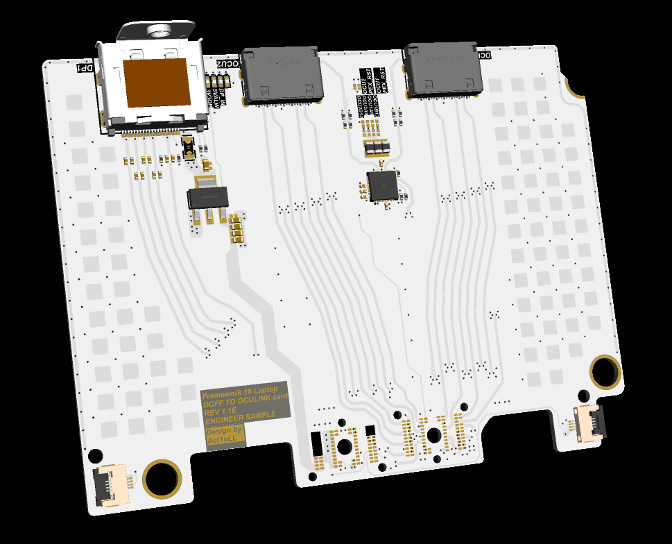
P.S. the reason this design is longer than the expansion bay is intentional. The Oculink port will on the back side of the PCB, to — enhance the signal strength.
Also the plastic/metal middle piece is removeable…
The design is, i would say 90% complete, and is about to get it printed and tested.