Don’t use my 2x4i design - it has errors.
I am not a PCB designer, but I tried since nobody else at the time seemed to.
Then J Cook came along and insisted he’d do it properly with a redriver (which I realistically would never be able to do). He had experience designing and selling parts for the FW already - and so I dropped my work. Sadly he then disappeared after taking some peoples money.
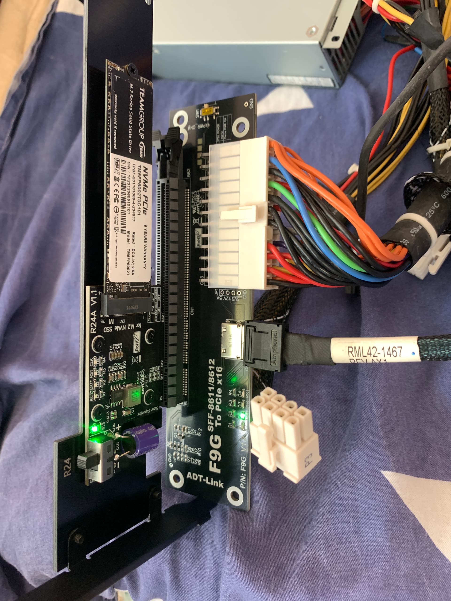
Now we all use the Dual M.2 Bay + Adapter version. It works fine, and I am currently too busy with another, frankly more important project of mine (AsterTrack) to realistically start working on this again.
A lot of my time (most of it honestly) working on this PCB has been spend fixing multilayer stuff in KiCAD (that also turned out to be wasted since the KiCAD devs just don’t care to merge it).
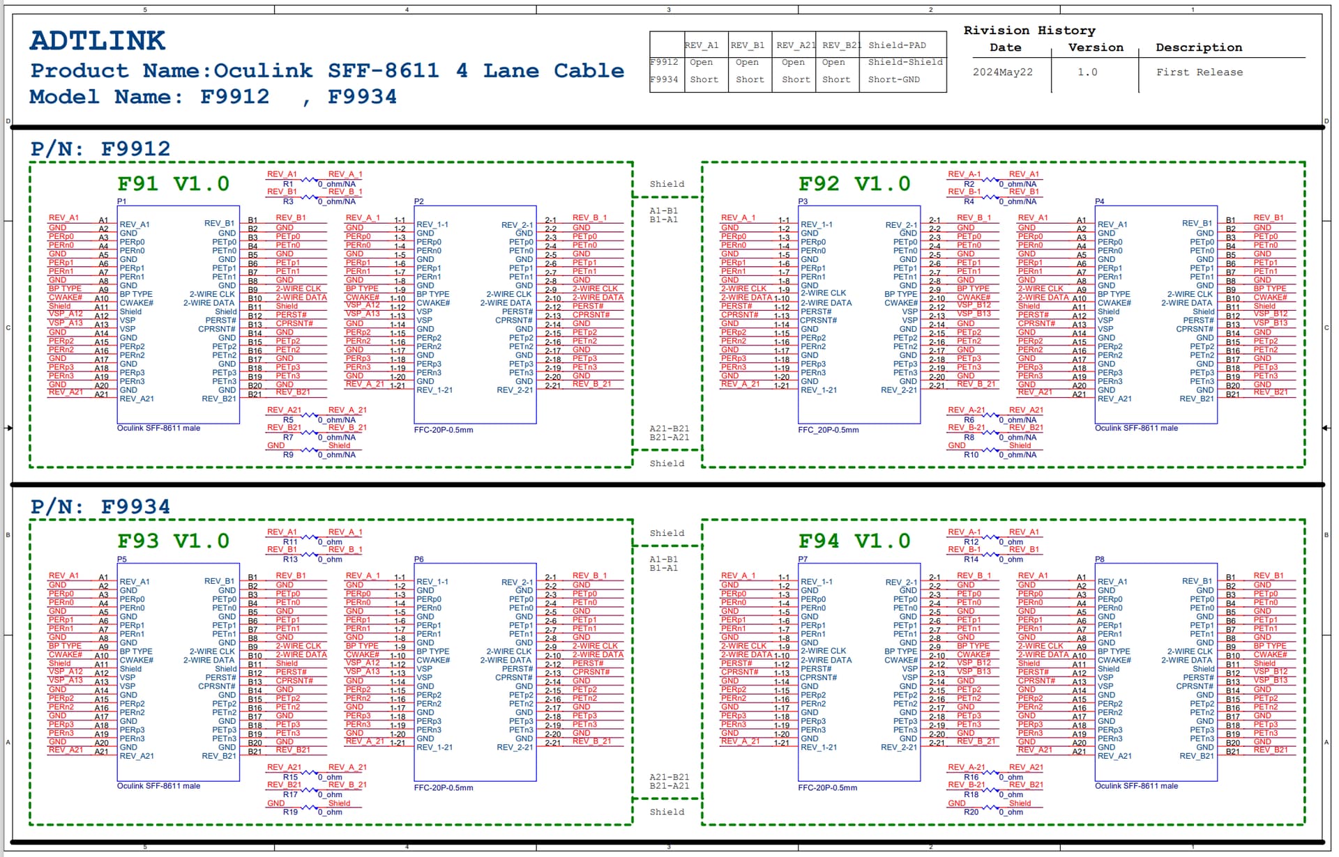
After the initial 4-layer 2x4i board you mentioned, I decided to focus on a 6layer 8i board (mostly to increase the chances the signal integrity works).
Your assessment is mostly correct. Two additions:
4) The DP in is only important for using the internal screen. Streaming to a wireless VR headset or even using Link over USB is not affected in the slightest. Even more so, I’m using a RX 6950XT on 4i and play on my internal screen, and honestly, it’s fine. No hard numbers on how much performance I lost (because it’d be meaningless, I have no windows install, and linux performance numbers aren’t consistently available). But honestly I think the DP in isn’t as big of an issue. I’d still aim to include it ofc.
6) I think you mean a redriver/retimer (different things). Yes it’s required - but surprisingly, it is fine if it’s in the eGPU dock. Given the DEG1 is relatively cheap at 100€, I’m of the opinion that any PCB design should skip a redriver and retimer, and just keep the signal integrity as good as possible. Chances are, as long as you don’t make it worse than the current mess of adapters, it’ll be fine with a DEG1. If you go 8i, you might want a redriver, because afaik there’s no 8i eGPU boards with a redriver - so that will get expensive.
So yeah, sorry to dissappoint, no chance I can spend the time on this personally in the near future. I wish I could, trust me. On the other hand, I came into this with no knowledge, but was able to gain that knowledge, and so can you. Learn KiCAD, watch this wonderful video (watch others first and return to it if it’s too dense for you right now), and you should have a good chance of doing this right.
If anybody wants my custom KiCad build along with the Custom DRC rules for the PCIe+DP routing on a JLC stackup that should allow for easy routing of a 4 or 6 layer PCB, DM me. It’ll still be a ton of work.