Sorry for letting you wait for so long! ![]()
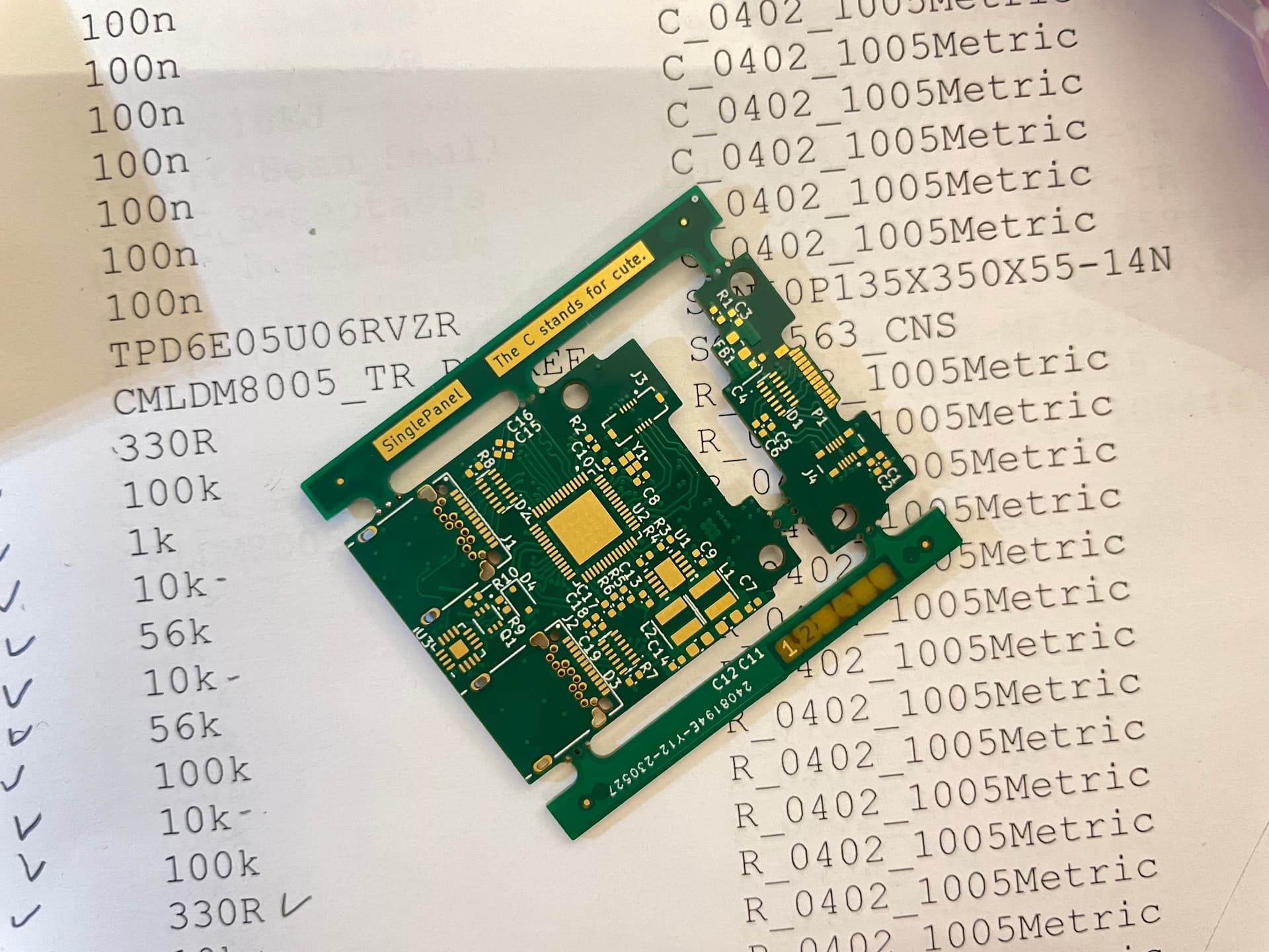
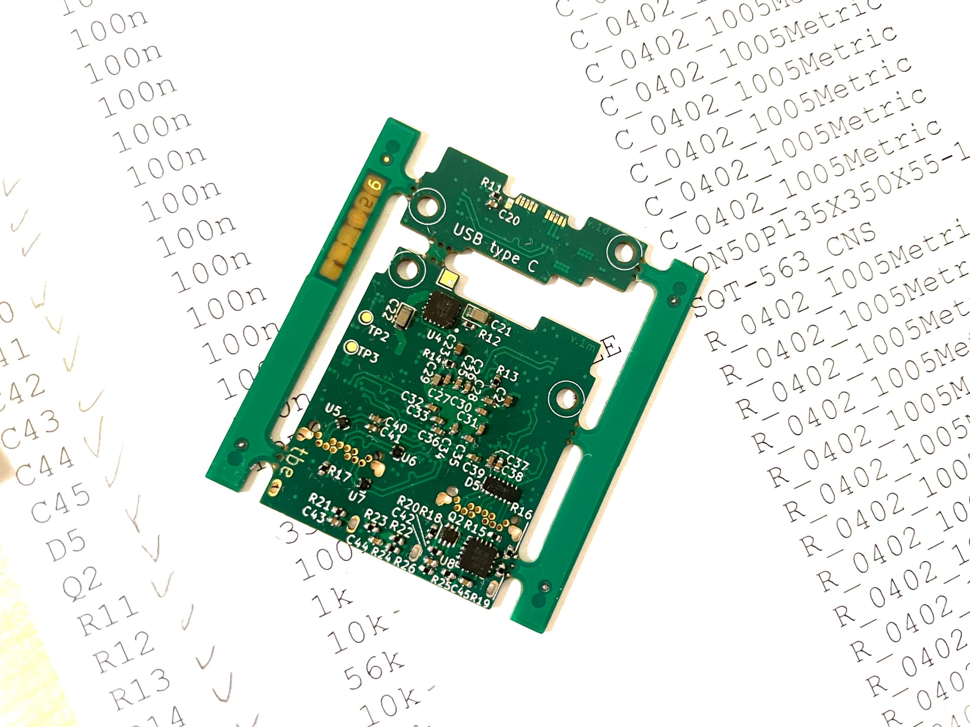
My design ended up being a 6-layer two part assembly, with one PCB having basically only the USB-C plug and a board-to-board connector on it to offset it in height. I made it a tiny panel to make handling easier.
It can most likely be simplified a little and made more producion-friendly.
I did actually assemble the first (bottom) side tonight, but I really have to go to bed now!
Still have to properly clean it and touch up a few spots.
The top side looks a little more exciting with the main IC, voltage converter and the connectors there but it’s not assembled yet. I’ll do that on the weekend. I hpoe it survives a second reflow cycle without components falling off ![]() .
.
Assembled bottom:
Bare top: