ooooh yeah, I’ve been there. Easy road to burnout. Please do be careful, we’ll be here no matter how long it takes! ![]()
4 Likes
Hi,
You might need the PRSNT# pins also connected.
I do think further diagnosis will be difficult without an oscilliscope.
You could then check eye patterns on the clk pins, and the link training patterns on the link pairs.
Unfortunately, not many pcie host chips give link training diagnostic info.
So, it is difficult to see at what stage the link negotiation failed.
The link training happens before pcie enumeration.
Does this help at all:
It is someone else that has done a pcie to mxm adapter.
*Dies internally.
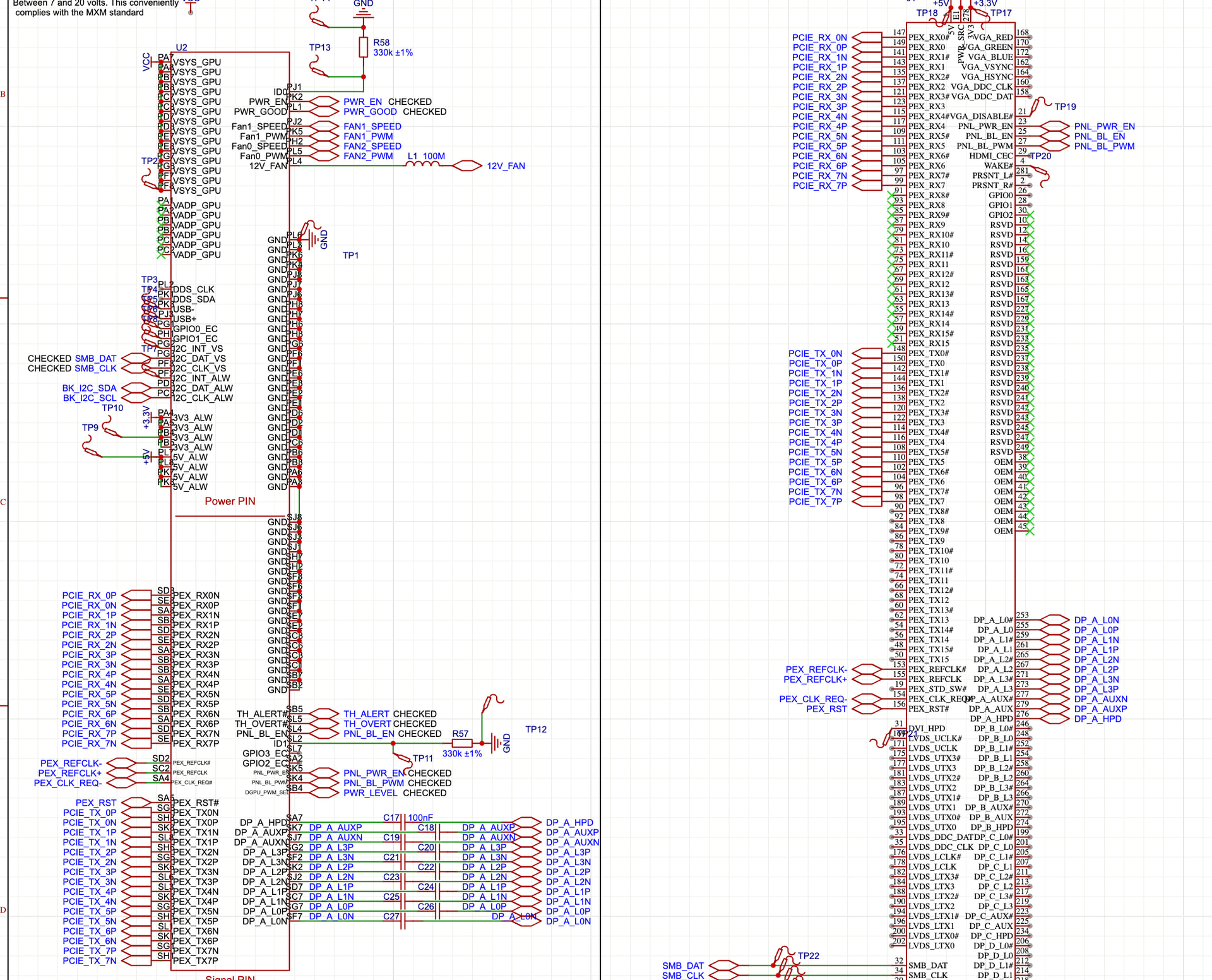
I think I’ve found the problem.
I think I’ve screwed up the PCIE lines. Again.
My schematic has TX0+ going to TX0+
![]()
![]()
But I don’t think this is right.
Because we’re not, “just passing signals through” - the pairs need to be swapped. I found another github repo where someone had started designing their own Framework to MXM board, (but hasn’t finished it yet), which had them the right way around, which is what triggered the train of thought.
I’m slightly in disbelief though.
Anyway, if someone could just confirm that yes, I’ve got them wrong , (and TX0P should go to TX0N), that would be great, and then I’ll fix the PCB and get another one ordered.
I’m sure everyone’s delighted that the guy whose designing the adapter for you to put an $1000 mobile 4090 card into got his left and right muddled. Twice.
Anyway, I’m happy to at least have found some source of the problem.
Thank you all so, so much for your patience,
JJ
7 Likes
It might be worth pointing out to FW that their documentation in this area is ambiguous at best. It is not very helpful, and it would be great if they could fix their documentation.
For example, if they mark something as “output”, they need to say if that is output from mainboard towards expansion bay, or visa versa.
Even better if:
They published the schematics for their nvme m.2 expansion bay card, as that would then be 100% unambiguous.
Note: there are other pcb developers making the same mistakes as you.
4 Likes
Thanks for the support. I meant to mention it already, but I’ve just finished writing a developer guide for the expansion bay in the Readme of Framework’s expansion bay page. I’ve submitted it as a pull request to try and get it published alongside all the existing documentation. You should be able to read it if you look inside the pull requests for the page, or if not I’ll publish it separately, but it covers things like how to set up the EEPROM and power delivery.
Give it a read and I’m really open to suggestions!
Link to the pull request is here you should be able to see the documentation in the Readme.
6 Likes
I have to say that the progress you’ve made on this project has been amazing! I love coming back here and seeing how much you have done. I think you’ll get it working and I can’t wait to see the finished product.
5 Likes
Hey everyone,
Quick update because it’s been a while.
I’ve finished routing all the PCIE traces for the new board, and just need to put the test points on before it should be ready for one final check and then send off.
Nothing more than that actually, but hope you’re all well ![]()
7 Likes
It’s done, (I hope).
V0.34 is live on github, if anyone wants to take a look.
Here’s the changelog:
- Significantly shrunk board design, (why? Because I’d rather prototype lots of cheap small boards than a few big ones)
- Significantly less complicated, especially when looking at EEPROM. All addresses are now just tied to ground, as I can’t think of any situation ever when I’d change them.
- Removed some unnecessary jumpers
- Made test points bigger for easier troubleshooting, and exposed points which were previously hidden underneath the card.
- Moved a couple of less critical components to the other side of the board to conserve space
- Fixed orientation of PCIE lines, (again), to match a-little-wifi’s design. Pretty sure this is correct now.
- Removed capacitors on PCIE lines.
A couple of things then before I put the order in:
- If anyone has any framework/open-source/interesting art they want to try putting on a pcb I’d be delighted to take images to put on the silkscreen.
- Having someone else just sanity check what I’ve done with the PCIE lines would be a great relief. I’d really rather not have to design this for a fourth time. The schematic is below to make it as easy as possible:
I’ll wait a few days for suggestions/fixes whatever the case.
Thanks everyone!
15 Likes
I’m loving all the progress you’re making on the module! It’s one of the only things I pop in the community forum to look at these days.
I found a preliminary listing for the RTX 5000 Pro Blackwell MXM GPU. Maybe I can use your module to power it someday! ![]()
6 Likes
Just put in the order. PCB prices are getting expensive!
I’m going to migrate over to KiCad for the next iteration of the board after many headaches with EasyEDA.
6 Likes
Hi.
In case you are still trying to get the pcie links the right way round.
There is an oculink board here that is tested working, so the pcie links must be right.
2 Likes
Just cross referenced - still happy with the routing. Thanks though for the info - also really impressive of @Filip to have finally brought the community through to the end of a two year long project. Very excited to see all the cool things that people make with it, and also incredibly useful as a reference document, (thanks for making it open source!).
5 Likes
Just to add if you did not already know as it was a recent discovery for me. You can swap the positive and negative sides of TX, RX and REFCLK however you want for easier routing (its a required part of the spec). That’s what I did for the currently working revision of the board and it has been working without any hiccups for the past 2 days. I’ll keep testing it for the next week or so to make sure it continues to be so.
I’m really happy that there’s finally a working solution as I have been waiting for this long before the first batch of the laptop shipped and since I got my first batch. All it took was for me to start reading up and learning to do more than just basic PCB routing (although this board is pretty basic since its just a passive adapter with fancy restrictions for the differential pairs. I was almost certain that I would need a redriver, or at worst a retimer, but somehow I am getting gen 4.0 without them, so I consider PCIe pretty forgiving in terms of signal integrity). I’m excited to see other solutions too.
EDIT: Also, the clock request and pcie reset signal are still routed pretty badly rn, which is what I’m currently fixing for the next revision of the board. So take extra caution with the way they are connected when referencing my design. (The PEX_RST signal also did not work and I had to use the SSD1 reset signal, so it was just a matter of moving the 0 Ohm resistor)
1 Like
Thanks for the info. This is actually slightly concerning though - shouldn’t that mean that the design I put down to having the traces the wrong way around should work?
What do you think could be the problem then?
If you connected lanes to their correct numbers and labels, that should work. Swapping p and n does not matter all, you can see how I have them in different orders if you were to look at my schematic. So doing that will definitely work no matter what. You just have to make sure the lanes are in correct order (0 to 0, 1 to 1… etc).
The issue I had with my board is that I used that PEX_RST (SA5 pin) signal and connected it to the PCIe reset signal on the OCuLink connector, which resulted in the whole PCIe handshake never starting and the boards not attempting to communicate. Now it is connected to PF3 which is the EXT_SSD1_RST signal and it immediately sprung to life. You should basically connect CLK_REQ to ground (at least in my case since OCuLink does not support this pin, I did this through a 1kOhm resistor, since the M.2 expansion card does the same when I looked at it with a multimeter) and the RST signals should connect to the corresponding RST signal on the device or port you’re connecting through. For the RST signals, I would just recommend pulling them all out and having a similar unpopulated resistor array. Best to have a way to connect different RST pins if one does not work… I feel so stupid that I did not do this for the first run of the board.
If I read it correctly, Filip was saying that wires in a pair can cross or not cross.
While if I understood your post, yoir issue was swapping TX nad RX pairs for the same number.
Edit: and I indeed understood your latest post wrongly. Then seems like it should work without swapping.
I read a bit more of the thread, but was the GPU you connected not detected at all in device manager? If it really was not detected at all, you might actually have the same issue like me and have used PEX_RST instead of EXT_SSD1_RST. I also see that in the recent schematic you posted.
My first line of thought before finding out about this on my board, is that I might have to swap my RX and TX lines, but thankfully I decided to “throw” money at the problem and first route all the RST and REQ signals to few test points and 0 Ohm resistor/jumper pads, so I can test with them. I would have otherwise tried swapping the lines if I didn’t get the board to work now.
EDIT: Also please don’t be like me and attempt to solder a tiny wire to one of the connector pads for the mainboard connector. I ruined 2 whole interposers with that as the difference in height due to solder on the pad with the wire would immediately bend the leg on the interposer without it springing back… and trying to bend it back makes it just snap lol.
1 Like
Hi.
One point that might be worth considering.
High frequency traces that pass very close to the edge of the PCB, or close to drilled holes in the PCB tend to under-perform. So, maybe try to move those traces a little.
2 Likes
So you’re saying that PCIE Reset should actually be connected to EXT_SSD1_RST, as opposed to PEX_RST? How come? But yes, my current schematic, (and the one I’ve just sent off to be manufactured *sigh*), uses PEX_RST. Thanks for all your help with this by the way.
Yes, that is what caused my first board to not work at all, for the 2nd revision I added resistor pads between all RST pins on the interposer connector to the RST pin of my oculink connector and just started to move a resistor to different pins, which is where SSD1_RST worked. I should be able to try different EEPROM data that was recently put onto Framework’s GitHub to test if PEX_RST starts working, but I have currently been unable to find the time to pull out my soldering equipment to move the single resistor lol. I did flash the new data onto the EEPROM and the resistor being on SSD1_RST still works, so I’m unsure if that made any change, but I’ll see if it keeps working when I move the resistor back to PEX_RST.
1 Like